Photonic integrated circuits
Also known as Photonic ICs, PICs, Silicon photonics chips
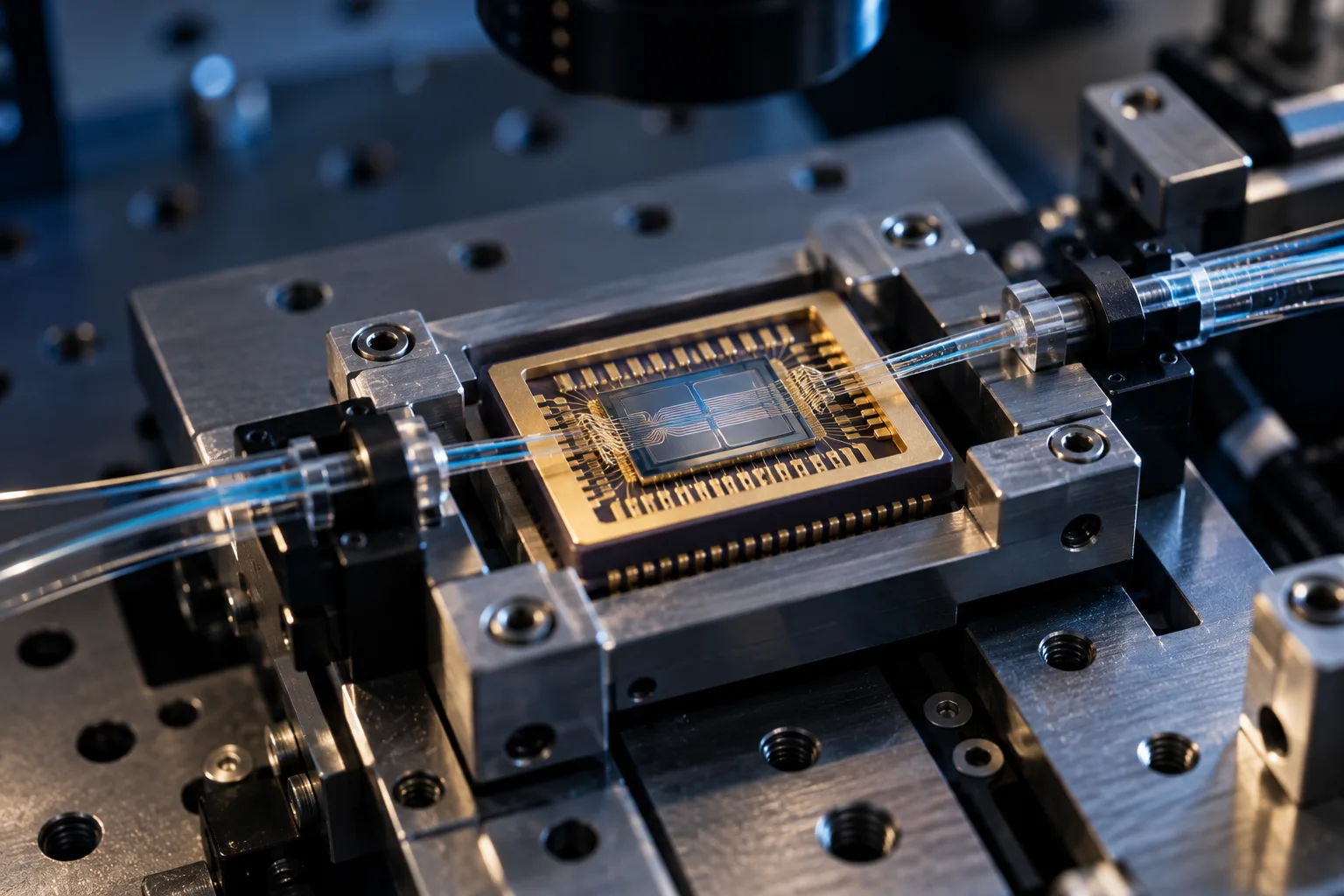
Photonic integrated circuits put lasers, waveguides, modulators and detectors on a single chip so that light, rather than only electricity, carries and processes signals. Silicon photonics has established foundry access, and Broadcom's 2025 co-packaged optics switch uses silicon photonics engines. Thin-film lithium niobate and indium phosphide serve other functions.
In plain language
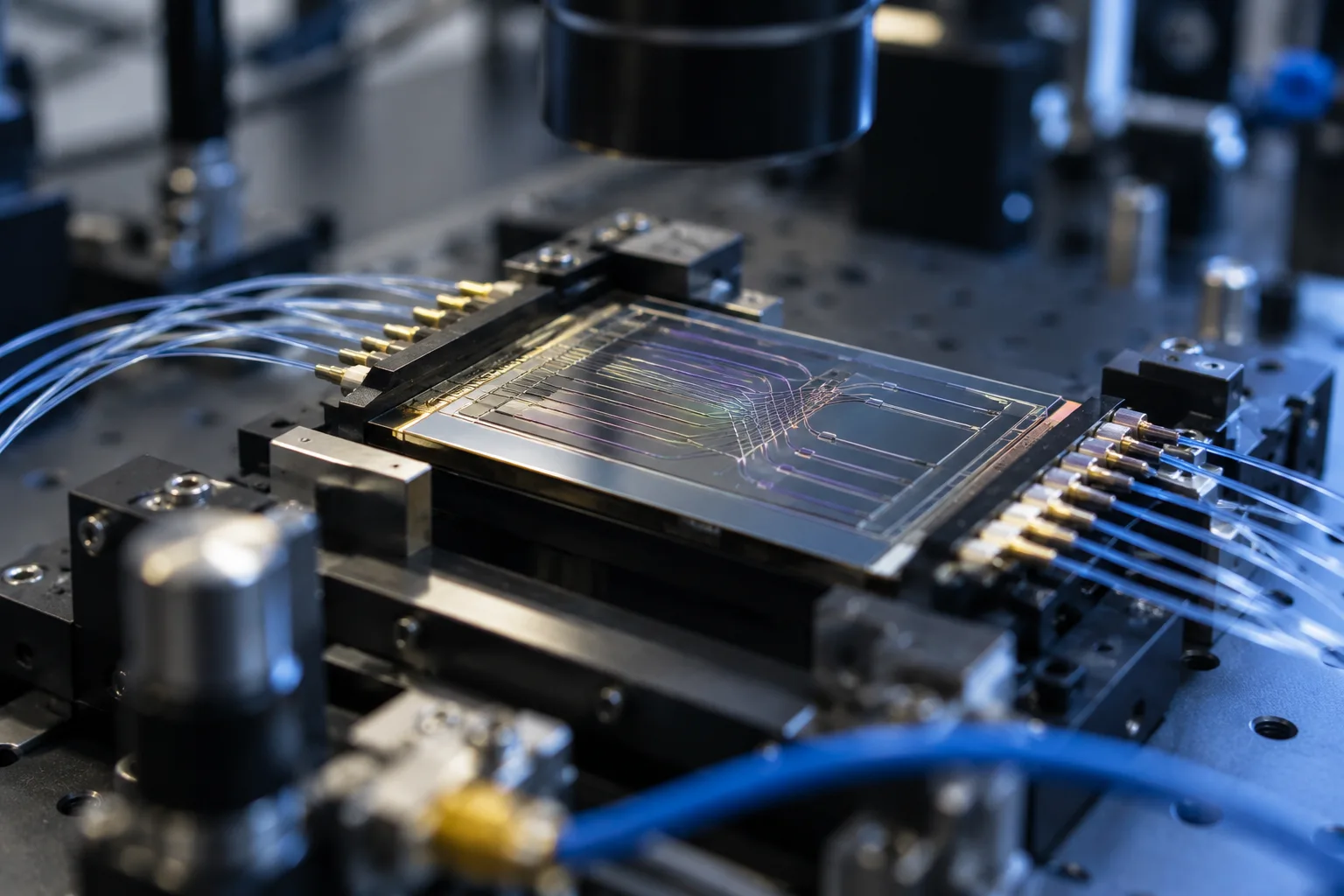
A photonic integrated circuit is a chip with tiny channels, called waveguides, that guide light the way wires guide electric current. Components such as light sources, switches, modulators (which encode data onto light) and detectors are built onto the same chip. Because the optical parts are made together in one process, a single chip can do work that would otherwise need many separate optical components.
The main reason these chips matter is data movement. Large data centres send huge volumes of information between servers and switches, and sending that information as light over short distances can reduce the energy and space needed per bit. Making the chips is not simple, though. Light has to be coupled in and out of very small waveguides, and the chip often needs a separate laser made from a different material, so packaging and assembly are widely described as the main cost and difficulty.
Technical explanation
Photonic integrated circuits (PICs) are built on several material platforms, each with different strengths. Silicon photonics uses silicon-on-insulator wafers and standard semiconductor processing, which lets it draw on the same wafer-scale manufacturing used for electronic chips. Silicon has weak native light emission, so lasers are usually made from III-V semiconductors and bonded onto the silicon. The imec iSiPP200 platform, for example, is a 200 mm silicon photonics process that supports silicon nitride waveguides and III-V lasers added by flip-chip bonding at wafer scale.
Thin-film lithium niobate (TFLN) is a separate platform. A 2021 review by Zhu, Shao, Lončar and colleagues reports that some thin-film devices, including modulators and wavelength converters, already outperform equivalents built from bulk crystal, and that ultra-low-loss resonators enable optical frequency combs and quantum transducers. Indium phosphide (InP) integrates light sources, amplifiers and modulators directly on one material. The EU-funded EUROPIC project set up a generic InP foundry for industrial use, with an InGaAsP platform for wavelengths of about 1.3 to 1.55 micrometres, and reported about 20 designs realised on the platform plus 5 external user designs.
Foundry access is a central part of the platform story. Most small users reach these chips through multi-project wafer (MPW) runs, in which several customers share one wafer and its fixed cost. Each foundry supplies a process design kit (PDK), a library of verified components that designers use in standard design tools. AIM Photonics, a US institute with a 300 mm foundry at the NY Creates Albany NanoTech Complex, offers multi-project wafer services and says the model lowers prototyping cost for a single buyer. Commercial demand is visible in data-centre optics, where silicon photonics is used in co-packaged optics (CPO), in which the optical engine sits in the same package as the switch chip. NVIDIA and Broadcom both announced CPO switches in 2025, and Broadcom's Tomahawk 6 Davisson is described as using sixteen 6.4 Tb/s silicon photonics engines.
What the evidence says
Each statement is typed by the strength of its evidence and linked to the source that supports it.
Demonstrated Shown in a published experiment, test or shipping product.
AIM Photonics offers multi-project wafer runs and its homepage describes a 300 mm foundry at the NY Creates Albany NanoTech Complex. It says the multi-project wafer model lowers prototyping cost for a single buyer.
Sources: [3] · Homepage, MPW and facility sections · medium confidenceimec's iSiPP200 is a 200 mm silicon photonics platform with a silicon-validated process design kit, supporting silicon nitride waveguides and III-V lasers added by flip-chip bonding at wafer scale.
Sources: [6] · iSiPP200 descriptionNVIDIA announced Spectrum-X Photonics and Quantum-X Photonics switches on 18 March 2025, which combine electronic switching with co-packaged optics.
Sources: [1] · Press release headline and first paragraphsSome thin-film lithium niobate devices, such as modulators and wavelength converters, already outperform equivalents built from bulk crystal, and ultra-low-loss resonators enable optical frequency combs and quantum transducers.
Sources: [4] · AbstractThe EU-funded EUROPIC project set up a generic indium phosphide foundry for industrial photonic chip production on an InGaAsP platform for wavelengths of about 1.3 to 1.55 micrometres, and reported about 20 application-specific designs plus 5 external user designs.
Sources: [5] · Progress and results sections · medium confidenceReported, unverified Stated by a company or team but not independently confirmed.
NVIDIA claims its photonic switches deliver 4x fewer lasers, 3.5x more power efficiency, 63x greater signal integrity, 10x better network resiliency at scale and 1.3x faster deployment, all compared with unspecified traditional methods.
Sources: [1] · Press release key claims · low confidenceBroadcom's Tomahawk 6 Davisson is a 102.4 Tb/s Ethernet switch with co-packaged optics, using sixteen 6.4 Tb/s silicon photonics optical engines.
Sources: [2] · Product description, paragraphs 1 and 3 · medium confidenceBroadcom executive Manish Mehta says Meta's testing of an earlier co-packaged optics generation showed a 5x improvement in serviceable failures over pluggable transceivers. Broadcom also claims link flap reductions for Davisson. The article gives no measured data for either claim.
Sources: [2] · Quoted product claims · low confidenceLimitations and open problems
- Vendor performance figures for co-packaged optics, from NVIDIA and Broadcom, are company claims. Their baselines are not defined in the sources reviewed, and no independent measurements were found.
- Packaging and fibre-to-chip coupling are widely described as the main cost and reliability limits. The sources reviewed here did not give verified loss or cost figures, so none are quoted.
- Silicon has weak native light emission, so lasers are usually made from III-V materials and bonded or integrated onto the chip. This adds process steps and cost.
- Shipment volumes for 800G and 1.6T silicon photonics transceivers could not be verified from open sources. Forecasts found were paywalled or unconfirmed.
- Multi-project wafer runs share one fabrication cycle, so users are limited to the components in the foundry's process design kit and to the run schedule, which can make custom devices harder to build.
Possible future uses
Ideas, not predictions. None of these has been demonstrated.
- Optical links between chips inside future AI computing clusters, where the optical engine sits beside each processor rather than at the rack edge.
- Thin-film lithium niobate modulators for high-speed communication and microwave signal processing in future network equipment.
- Small quantum photonic chips built through low-cost multi-project wafer runs by university and start-up teams.
Timeline
- 2011First application-specific photonic integrated circuits from the EUROPIC generic indium phosphide multi-project wafer runs become available. Sources: [5]
- 2021Zhu, Shao, Lončar and colleagues publish a review of thin-film lithium niobate integrated photonics in Advances in Optics and Photonics. Sources: [4]
- 18 Mar 2025NVIDIA announces Spectrum-X Photonics and Quantum-X Photonics switches built with co-packaged silicon photonics optics. Sources: [1]
- 9 Oct 2025Broadcom's third-generation co-packaged optics Ethernet switch, Tomahawk 6 Davisson, rated at 102.4 Tb/s, is reported with sixteen 6.4 Tb/s optical engines. Sources: [2]
Futures this could help bring about
Glossary
- Waveguide
- A narrow channel, typically a few hundred nanometres wide on a chip, that guides light along a path.
- Silicon photonics
- Making optical components on silicon wafers using semiconductor manufacturing methods, so that they can be produced at scale.
- Co-packaged optics
- Placing optical engines in the same package as a switch or processor chip, so the electrical link between them is shorter.
- Multi-project wafer (MPW)
- A shared fabrication run in which several customers' designs are placed on one wafer to share the cost.
- Process design kit (PDK)
- A library of verified components and rules that lets designers lay out photonic chips in standard design software.
Sources
- company announcement
NVIDIA Announces Spectrum-X Photonics Co-Packaged Optics Networking Switches to Scale AI Factories to Millions of GPUs
NVIDIA Investor Relations, 18 Mar 2025. Accessed 21 Oct 2026. - news
Broadcom bets big on AI with new CPO
Ben Wodecki. SDxCentral, 9 Oct 2025. Accessed 21 Oct 2026. - other
AIM Photonics homepage (undated home page; date shown is its latest news item)
AIM Photonics, 20 Oct 2026. Accessed 21 Oct 2026. - review article
Integrated photonics on thin-film lithium niobate
Di Zhu, Linbo Shao, Mengjie Yu et al.. Advances in Optics and Photonics, 2021. DOI: 10.1364/AOP.411024. Accessed 21 Oct 2026. - government report
European Manufacturing Platform For Photonic Integrated Circuits (EUROPIC): final report summary
European Commission, CORDIS, Jul 2012. Accessed 21 Oct 2026. - other
imec photonics: development and offer
imec, 21 Oct 2026. Accessed 21 Oct 2026.
Revision history
3 changes since this profile was created.