2D semiconductor electronics
Also known as 2D semiconductors, Two-dimensional semiconductor transistors, MoS2 transistors, Atomically thin transistors
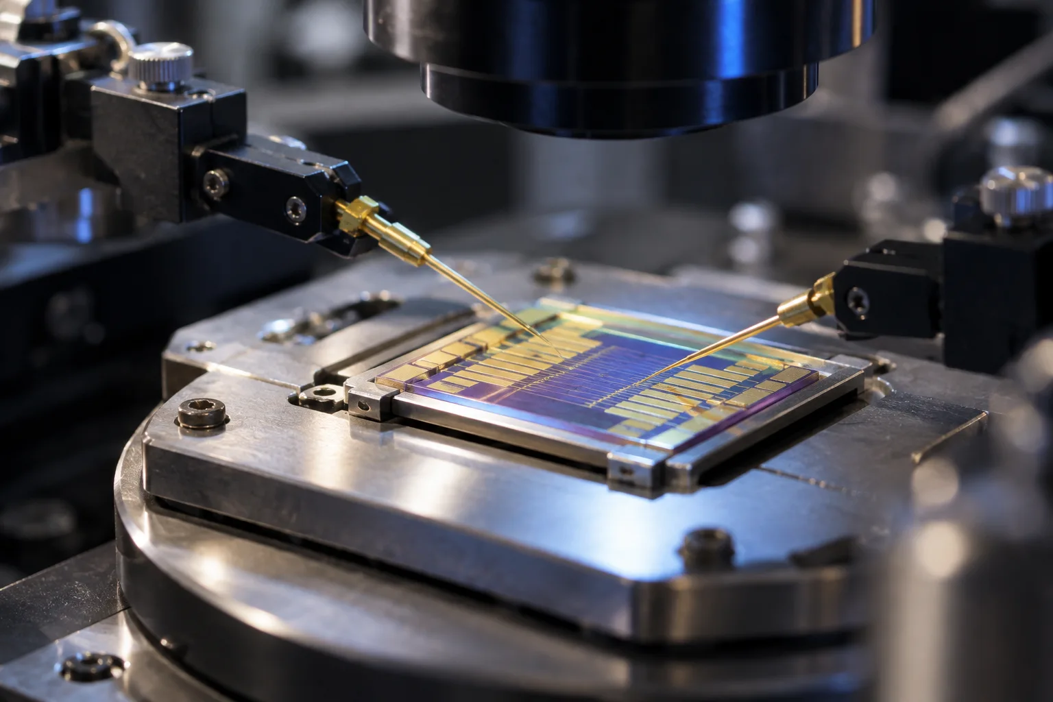
Two-dimensional semiconductors such as molybdenum disulfide (MoS2) form sheets only a few atoms thick and could make transistors that keep working at very small sizes. Lab devices and a small 1-bit processor have been demonstrated, but no production chips built from these materials are described in the sources reviewed here.
In plain language
A computer chip is built from millions of transistors, which act as tiny switches. As transistors shrink, the silicon channel that carries current becomes harder to control, and the switch leaks when it should be off. Researchers are testing sheet-like materials, only a few atoms thick, as an alternative channel that may stay controllable at smaller sizes.
The best-known example is molybdenum disulfide, or MoS2, which is similar to the graphite in a pencil but forms a single layer that is very thin. In 2011, a lab study showed single-layer MoS2 transistors that switched on and off with a very high ratio at room temperature. In 2017, a research group built a simple 1-bit processor from MoS2 transistors, but the sources reviewed here describe lab devices rather than chips sold for use in products.
Technical explanation
Single-layer molybdenum disulfide has a direct bandgap, which lets it switch current on and off in a transistor. Radisavljevic and colleagues (2011) reported single-layer MoS2 transistors with a hafnium oxide gate dielectric, reporting room-temperature mobility of at least 200 square centimetres per volt-second and on/off current ratios of about 10^8 at room temperature, with very low standby power. The authors also noted that the direct bandgap could suit interband tunnel transistors with lower power consumption.
Scaling has been pushed further in single devices. Desai and colleagues (2016) reported a MoS2 transistor with a 1 nm physical gate length, using a single-walled carbon nanotube as the gate electrode. Wachter and colleagues (2017) built a 1-bit microprocessor from 115 MoS2 transistors that could run user-defined programs held in external memory. The authors describe it as the most complex circuit built from a 2D material at that time.
Measuring progress is not straightforward. Liu and colleagues (2021), in a Nature perspective, argue that common metrics such as carrier mobility and contact resistance can be misestimated, and they propose saturation or on-state current density, especially in the short-channel limit, as more reliable benchmarks for comparing 2D semiconductors.
What the evidence says
Each statement is typed by the strength of its evidence and linked to the source that supports it.
Demonstrated Shown in a published experiment, test or shipping product.
Single-layer MoS2 transistors with a hafnium oxide gate dielectric reached room-temperature mobility of at least 200 square centimetres per volt-second and on/off current ratios of about 10^8 in a laboratory study.
Sources: [1] · medium confidenceA MoS2 transistor with a 1 nm physical gate length and a single-walled carbon nanotube as the gate electrode was reported in Science in 2016.
Sources: [2] · AbstractA 1-bit microprocessor built from 115 MoS2 transistors can run user-defined programs stored in external memory and communicate with peripheral devices.
Sources: [3] · AbstractReported, unverified Stated by a company or team but not independently confirmed.
The 115-transistor MoS2 microprocessor is described by its authors as the most complex circuit built from a 2D material at the time of publication.
Sources: [3] · medium confidenceProposed A design or plan that has not yet been built or tested.
The authors state that the direct bandgap of a monolayer MoS2 could be used to build interband tunnel transistors with lower power consumption than classical transistors.
Sources: [1] · medium confidenceLiu and colleagues argue that metrics such as carrier mobility and contact resistance can be misestimated for 2D transistors, and propose saturation or on-state current density, especially in the short-channel limit, as more reliable benchmarks.
Sources: [4] · medium confidenceLimitations and open problems
- The sources reviewed describe laboratory transistors and one small lab processor; none describe production chips built from 2D semiconductors.
- Contact resistance between metal electrodes and the 2D channel is a central problem and can distort device comparisons (Liu and colleagues, 2021).
- Reported mobility and on-state current depend on how they are measured, so figures from different papers need careful comparison (Liu and colleagues, 2021).
- The 1-bit, 115-transistor processor is far simpler than the silicon processors used in computers.
- Results from single devices do not show that large areas of uniform 2D semiconductor can be made reliably.
Possible future uses
Ideas, not predictions. None of these has been demonstrated.
- Ultra-thin transistors for flexible or wearable electronics, such as electronic skin.
- Energy-efficient interband tunnel transistors using the direct bandgap of a single MoS2 layer, as suggested by Radisavljevic and colleagues (2011).
- Stacked layers in which 2D transistors are built on top of conventional silicon circuits to add functions without enlarging the chip.
Timeline
- 30 Jan 2011Single-layer MoS2 transistors with room-temperature on/off current ratios of about 10^8 are reported in Nature Nanotechnology (lab devices). Sources: [1]
- 7 Oct 2016A MoS2 transistor with a 1 nm physical gate length is reported in Science. Sources: [2]
- 11 Apr 2017A 1-bit microprocessor built from 115 MoS2 transistors is reported in Nature Communications. Sources: [3]
- 3 Mar 2021Nature publishes a perspective arguing that common benchmarks for 2D transistors, including mobility and contact resistance, can be misestimated. Sources: [4]
Futures this could help bring about
Related breakthroughs
Glossary
- Transistor
- A small electronic switch that controls the flow of current; chips contain millions or billions of them.
- On/off ratio
- The ratio of current when a transistor is switched on to the current when it is switched off; higher values mean clearer switching.
- Contact resistance
- Electrical resistance where a metal electrode meets the semiconductor channel; it adds losses that limit device performance.
- Two-dimensional (2D) material
- A material formed as a single layer or a few layers of atoms, such as molybdenum disulfide.
Sources
- peer reviewed paper
Single-layer MoS2 transistors
B. Radisavljevic, A. Radenovic, J. Brivio et al.. Nature Nanotechnology, 30 Jan 2011. DOI: 10.1038/nnano.2010.279. Accessed 21 Oct 2026. - peer reviewed paper
MoS2 transistors with 1-nanometer gate lengths
Sujay B. Desai, Surabhi R. Madhvapathy, Angada B. Sachid et al.. Science, 7 Oct 2016. DOI: 10.1126/science.aah4698. Accessed 21 Oct 2026. - peer reviewed paper
A microprocessor based on a two-dimensional semiconductor
Stefan Wachter, Dmitry K. Polyushkin, Ole Bethge et al.. Nature Communications, 11 Apr 2017. DOI: 10.1038/ncomms14948. Accessed 21 Oct 2026. - review article
Promises and prospects of two-dimensional transistors
Yuan Liu, Xidong Duan, Hyeon-Jin Shin et al.. Nature, 3 Mar 2021. DOI: 10.1038/s41586-021-03339-z. Accessed 21 Oct 2026.